Most modern electronic devices practically do not use analog (transformer) power supplies; they have been replaced by pulse converters voltage. To understand why this happened, it is necessary to consider design features, as well as the strengths and weaknesses of these devices. We will also talk about the purpose of the main components of pulsed sources and give a simple example of an implementation that can be assembled with your own hands.
Design features and operating principle
Of the several methods of converting voltage to power electronic components, two that are most widespread can be identified:
- Analog, the main element of which is a step-down transformer, in addition to its main function, it also provides galvanic isolation.
- Impulse principle.
Let's look at how these two options differ.
PSU based on a power transformer
Let's consider a simplified block diagram of this device. As can be seen from the figure, a step-down transformer is installed at the input, with its help the amplitude of the supply voltage is converted, for example, from 220 V we get 15 V. The next block is a rectifier, its task is to convert the sinusoidal current into a pulsed one (the harmonic is shown above the symbolic image). For this purpose, rectifying semiconductor elements (diodes) connected via a bridge circuit are used. Their operating principle can be found on our website.
The next block performs two functions: it smoothes the voltage (a capacitor of appropriate capacity is used for this purpose) and stabilizes it. The latter is necessary so that the voltage does not “drop” when the load increases.
The given block diagram is greatly simplified; as a rule, a source of this type contains input filter and protective circuits, but this is not important for explaining the operation of the device.
All the disadvantages of the above option are directly or indirectly related to the main design element - the transformer. Firstly, its weight and dimensions limit miniaturization. In order not to be unfounded, we will use as an example a step-down transformer 220/12 V with a rated power of 250 W. The weight of such a unit is about 4 kilograms, dimensions are 125x124x89 mm. You can imagine how much a laptop charger based on it would weigh.
Secondly, the price of such devices is sometimes many times higher than the total cost of the other components.
Pulse devices
As can be seen from the block diagram shown in Figure 3, the operating principle of these devices differs significantly from analog converters, primarily in the absence of an input step-down transformer.
 Figure 3. Structural scheme pulse block nutrition
 Let's consider the operating algorithm of such a source:
- Power is supplied to the network filter; its task is to minimize network noise, both incoming and outgoing, that arises as a result of operation.
- Next, the unit for converting sinusoidal voltage into pulsed constant voltage and a smoothing filter come into operation.
- At the next stage, an inverter is connected to the process; its task is related to the formation of rectangular high-frequency signals. Feedback to the inverter is carried out through the control unit.
- The next block is IT, it is necessary for automatic generator mode, supplying voltage to the circuit, protection, controller control, as well as the load. In addition, the IT task includes ensuring galvanic isolation between high and low voltage circuits.
Unlike a step-down transformer, the core of this device is made of ferrimagnetic materials, this contributes to the reliable transmission of RF signals, which can be in the range of 20-100 kHz. A characteristic feature of IT is that when connecting it, the inclusion of the beginning and end of the windings is critical. The small dimensions of this device make it possible to produce miniature devices; an example is the electronic harness (ballast) of an LED or energy-saving lamp.

- Next, the output rectifier comes into operation, since it works with high-frequency voltage; the process requires high-speed semiconductor elements, so Schottky diodes are used for this purpose.
- At the final phase, smoothing is performed on an advantageous filter, after which voltage is applied to the load.
Now, as promised, let’s look at the operating principle of the main element of this device – the inverter.
How does an inverter work?
RF modulation can be done in three ways:
- pulse-frequency;
- phase-pulse;
- pulse width.
In practice, the last option is used. This is due both to the simplicity of implementation and to the fact that PWM has a constant communication frequency, unlike the other two modulation methods. A block diagram describing the operation of the controller is shown below.
The operating algorithm of the device is as follows:
The reference frequency generator generates a series of rectangular signals, the frequency of which corresponds to the reference one. Based on this signal, a sawtooth U P is formed, which is supplied to the input of the comparator K PWM. The UUS signal coming from the control amplifier is supplied to the second input of this device. The signal generated by this amplifier corresponds to the proportional difference U P ( reference voltage) and U PC (regulating signal from the feedback circuit). That is, the control signal UUS is, in fact, a mismatch voltage with a level that depends on both the current on the load and the voltage on it (U OUT).
This implementation method allows you to organize a closed circuit that allows you to control the output voltage, that is, in fact, we are talking about a linear-discrete functional unit. Pulses are generated at its output, with a duration depending on the difference between the reference and control signals. Based on it, a voltage is created to control the key transistor of the inverter.
The process of stabilizing the output voltage is carried out by monitoring its level; when it changes, the voltage of the control signal U PC changes proportionally, which leads to an increase or decrease in the duration between pulses.
As a result, the power of the secondary circuits changes, which ensures stabilization of the output voltage.
To ensure safety, galvanic isolation between the power supply and feedback is required. As a rule, optocouplers are used for this purpose.
Strengths and weaknesses of pulsed sources
If we compare analog and pulse devices of the same power, the latter will have the following advantages:
- Small size and weight due to the absence of a low-frequency step-down transformer and control elements that require heat removal using large radiators. Thanks to the use of high-frequency signal conversion technology, it is possible to reduce the capacitance of the capacitors used in the filters, which allows the installation of smaller elements.
- Higher efficiency, since the main losses are caused only by transient processes, while in analog circuits a lot of energy is constantly lost during electromagnetic conversion. The result speaks for itself, increasing efficiency to 95-98%.
- Lower cost due to the use of less powerful semiconductor elements.
- Wider input voltage range. This type of equipment is not demanding in terms of frequency and amplitude; therefore, connection to networks of various standards is allowed.
- Availability of reliable protection against short circuits, overload and other emergency situations.
The disadvantages of pulse technology include:
The presence of RF interference is a consequence of the operation of the high-frequency converter. This factor requires the installation of a filter that suppresses interference. Unfortunately, its operation is not always effective, which imposes some restrictions on the use of devices of this type in high-precision equipment.
Special requirements for the load, it should not be reduced or increased. As soon as the current level exceeds the upper or lower threshold, the output voltage characteristics will begin to differ significantly from the standard ones. As a rule, manufacturers (even recently Chinese ones) provide for such situations and install appropriate protection in their products.
Scope of application
Almost all modern electronics are powered from blocks of this type, as an example:


Assembling a switching power supply with your own hands
Let's consider the circuit of a simple power supply, where the above-described principle of operation is applied.

Designations:
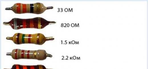
- Resistors: R1 – 100 Ohm, R2 – from 150 kOhm to 300 kOhm (selectable), R3 – 1 kOhm.
- Capacities: C1 and C2 – 0.01 µF x 630 V, C3 -22 µF x 450 V, C4 – 0.22 µF x 400 V, C5 – 6800-15000 pF (selectable), 012 µF, C6 – 10 µF x 50 V, C7 – 220 µF x 25 V, C8 – 22 µF x 25 V.
- Diodes: VD1-4 - KD258V, VD5 and VD7 - KD510A, VD6 - KS156A, VD8-11 - KD258A.
- Transistor VT1 – KT872A.
- Voltage stabilizer D1 - microcircuit KR142 with index EH5 - EH8 (depending on the required output voltage).
- Transformer T1 - a w-shaped ferrite core with dimensions 5x5 is used. The primary winding is wound with 600 turns of wire Ø 0.1 mm, the secondary (pins 3-4) contains 44 turns Ø 0.25 mm, and the last winding contains 5 turns Ø 0.1 mm.
- Fuse FU1 – 0.25A.
The setting comes down to selecting the values of R2 and C5, which ensure excitation of the generator at input voltage 185-240 V.
The inverter in the TV is a device for starting and stable operation fluorescent lamps LCD panel backlight. Ensures the constant glow of these light sources for a long time and effectively controls their brightness. It can be made in the form of one or two separate blocks (master/slave), and also located together with the power supply on a single board. If you do it yourself, you need to know the functions it performs.
Tasks of the television inverter:
- conversion of direct voltage 12 - 24 volts into high-voltage alternating voltage
- stabilization and adjustment of lamp current
- backlight brightness adjustment
- providing protection against overloads and short circuits
Electrical circuit of a simple inverter for 2 backlight lamps

![]() The device is implemented on a PWM controller U1 (OZ960), two assemblies of field-effect transistor switches (u1, u2) and high-voltage transformers T1, T2. Connector CN1 supplies 12 volt power (F1), a power command (ON/OFF), and constant pressure(Dimm) to adjust brightness. The protection unit (D2, D4, D5, D6) analyzes the current or voltage at the output of the device and generates overload and feedback voltages (OS) supplied to the PWM. If one of these voltages exceeds the threshold value, the oscillator at U1 is blocked, and the inverter will be in a protection state. The node is blocked when the supply voltage is low, when the supply voltage “drops” when the load is turned on, when the converter is overloaded or there is a short circuit.
The device is implemented on a PWM controller U1 (OZ960), two assemblies of field-effect transistor switches (u1, u2) and high-voltage transformers T1, T2. Connector CN1 supplies 12 volt power (F1), a power command (ON/OFF), and constant pressure(Dimm) to adjust brightness. The protection unit (D2, D4, D5, D6) analyzes the current or voltage at the output of the device and generates overload and feedback voltages (OS) supplied to the PWM. If one of these voltages exceeds the threshold value, the oscillator at U1 is blocked, and the inverter will be in a protection state. The node is blocked when the supply voltage is low, when the supply voltage “drops” when the load is turned on, when the converter is overloaded or there is a short circuit.
Characteristic signs of inverter malfunction
- Backlights do not turn on
- Backlights turn on and off briefly
- Unstable brightness and screen flickering
- The inverter periodically does not turn on after a long period of inactivity
- Uneven screen illumination with a 2-inverter circuit
Features of inverter unit repair
 When diagnosing faults related to the correct operation of the inverter, you should first of all make sure that there is no ripple in the supply voltage and that it is stable. Pay attention to the passage of startup commands and backlight brightness control from the motherboard. Eliminate the influence of backlight lamps by using their equivalent in cases where the problem is not clear. Take advantage of the opportunity to remove protection from the inverter during repairs to determine the defective part. Do not forget about a careful visual inspection of the board and what every professional TV technician uses when repairing TVs at home - measuring voltage, resistance, capacitance using special instruments or a tester.
Sometimes, upon careful inspection of the board, you can see “burnt out” parts that need to be replaced. Very often field-effect transistor switches fail, but sometimes replacing them does not always lead to a positive result. The functionality of the unit may be restored for an indefinite period of time, and then the malfunction may occur again. You have eliminated the effect, but not the cause. Therefore, without knowing the intricacies of repairing these devices, you can lose a lot of time and effort to restore them. And, if you have doubts about the success of the matter, call a technician who has already repaired similar devices many times and knows all the “pitfalls and shoals” thanks to his accumulated experience and professional knowledge.
![]() High-voltage transformers are considered the weak link in the inverter units. Working in conditions high voltage requires special assembly quality of these components and imposes high requirements to insulation properties. In addition, it should be said that transformers can become noticeably heated during the operation of the backlight. Defects such as a break or inter-turn short circuit of the windings of these parts are commonplace. Diagnostics of these elements can be complicated by the fact that a short circuit or break can only be observed in operating mode, and “diagnosis” of them in a de-energized state will not reveal problems with them. Here, swapping the dubious and serviceable transformer and further analyzing the situation can come to the rescue.
High-voltage transformers are considered the weak link in the inverter units. Working in conditions high voltage requires special assembly quality of these components and imposes high requirements to insulation properties. In addition, it should be said that transformers can become noticeably heated during the operation of the backlight. Defects such as a break or inter-turn short circuit of the windings of these parts are commonplace. Diagnostics of these elements can be complicated by the fact that a short circuit or break can only be observed in operating mode, and “diagnosis” of them in a de-energized state will not reveal problems with them. Here, swapping the dubious and serviceable transformer and further analyzing the situation can come to the rescue.
 Different TVs use inverters with different numbers of transformers. In small-sized devices, the inverter can contain 2 - 4 transformers; in large-diagonal TVs, especially of previous years of production, there were up to 20 similar products. Naturally, a large number of them reduces the reliability of the circuit as a whole, so in modern models their use is reduced to a minimum through innovative technical solutions.
A sign of an inverter malfunction in most cases is the absence of an image on the TV screen when there is sound. However, situations are possible when the TV, after trying to turn on, goes back into standby mode or starts flashing the LEDs on the front panel, and in this case no sound appears. The nature of the defect is different, and the source may still be the same inverter unit. Some TV models contain a feedback signal from the inverter to the motherboard processor, indicating malfunctions in its operation. Without receiving confirmation from the inverter that everything is fine with it, the processor changes the TV operating mode to standby or displays error messages via LED indicators. For some manufacturers, after a certain number of unsuccessful starts, the system may stop sending a command to turn on the backlight until errors are reset or the memory is cleared.
 The inverter is a complex electronic device, do-it-yourself repair which may cause certain difficulties. These blocks for TVs with diagonals from 26 inches and above are “tied” to a specific LCD panel and, according to manufacturers, are a single device (together with the T-con block). It is very rare to find electronic circuits for these products, and never for a matrix controller. Therefore, even a professional, when diagnosing this equipment, has to remember the experience of repairing similar devices and be guided general principles their circuit design solutions and use the database of datasheets for backlight driver chips and key transistors. If you decide to repair the inverter yourself, but something goes wrong,
Preface
I would like to warn dear readers of this article in advance that this article will have a form and content that is not entirely familiar to readers. Let me explain why.
The material presented to your attention is absolutely exclusive. All devices that will be discussed in my articles are developed, modeled, configured and brought to mind by me personally. Most often it all starts with an attempt to implement some kind of interesting idea. The path can be very thorny, and sometimes takes quite a long time, and what the final result will be, and whether there will be one at all, is not known in advance. But practice confirms that the one who walks will master the road... and the results sometimes exceed all expectations... And how fascinating the process itself is - words cannot express it. I must admit that I (like everyone else, it should be noted) do not always have enough knowledge and skills, and wise and timely advice is welcome and helps bring the idea to its logical conclusion. This is the specificity...
This article is addressed not so much to beginners, but rather to people who already have necessary knowledge and experience, who are also interested in walking untrodden paths, and for whom standard approaches to solving problems are not so interesting... It is important to understand that this is not material for thoughtless repetition, but rather the direction in which to move... I do not promise readers much detail about the obvious, well-known and things that are understandable to those literate in electronics..., but I promise that the main ESSENCE will always be well covered.
About the inverter
The inverter that will be discussed was born in exactly the manner described above... Unfortunately, I cannot, without violating the rules for publishing these articles, cover in detail how it came into being, but I assure you that the circuits of the two extreme versions of the inverter are not yet available anywhere have been published...Moreover, the penultimate version of the scheme is already practically in use, and the extreme one (I hope the most perfect of them) has not yet been mocked up only on paper, but I have no doubt about its functionality, and its production and testing will take only a couple of days...
Getting acquainted with the microcircuit for the half-bridge inverter IR2153 made a good impression - a fairly small current consumed by the power supply, the presence of a dead time, built-in power control... But it has two significant drawbacks - there is no ability to adjust the duration of the output pulses and a rather small driver current... (in reality, it is not stated in the datasheet, but it is unlikely that it is more than 250-500 mA...). It was necessary to solve two problems - to figure out how to implement voltage regulation of the inverter, and how to increase the current of the power switch drivers...
These problems were solved by introducing field-effect transistors into the optical driver circuit, and differentiating circuits at the outputs of the IR2153 microcircuit (see Fig. 1)
Fig.1
A few words about how adjusting the pulse duration works. Pulses from the outputs of IR2153 are supplied to differentiating circuits consisting of elements C2, R2, optical driver LED, VD3-R4 - optocoupler transistor..., and elements C3, R3, optical driver LED, VD4-R5 - optocoupler transistor... The elements of the differentiating circuits are designed in this way that, with the feedback optocoupler transistor closed, the duration of the pulses at the outputs of the optical drivers is almost equal to the duration of the pulses at the outputs of IR2153. At the same time, the voltage at the inverter output is maximum.
At the moment when the voltage at the inverter output reaches the stabilization voltage, the optocoupler transistor begins to open slightly... this leads to a decrease in the time constant of the differentiating circuit, and, as a consequence, to a decrease in the duration of the pulses at the output of the optical drivers. This ensures voltage stabilization at the inverter output. Diodes VD1, VD2 eliminate the negative surge that occurs during differentiation.
I deliberately do not mention the type of optical drivers. That's why the optical driver of a field-effect transistor is a big separate topic for discussion. Their range is very large - dozens... if not hundreds of types... for every taste and color. To understand their purpose and their features, you need to study them yourself.
The presented inverter has another important feature. Let me explain. Since the main purpose of the inverter is to charge lithium batteries (although any batteries can be used, of course), measures had to be taken to limit the current at the inverter output. The fact is that if you connect a discharged battery to the power supply, the charging current can exceed all reasonable limits... To limit the charging current to the level we need, a shunt Rsh is introduced into the control electrode circuit TL431... How does it work? The minus of the battery being charged is connected not to the minus of the inverter, but to the upper terminal of the circuit Rsh... When current flows through Rsh, the potential on the control electrode TL431... increases, which leads to a decrease in the voltage at the output of the inverter, and, as a consequence, to limiting the charging current. As the battery charges, the voltage on it increases, but after it, the voltage at the inverter output also increases, tending to the stabilization voltage. In short, it’s a simple and outrageously effective contraption. By changing the Rsh rating, it is easy to limit the charge current at any level we need. That is why the Rsh rating itself is not announced... (the reference value is 0.1 Ohm and below...), it is easier to select it experimentally.
Anticipating a lot of didactic comments about the “rights” and “wrongs” of charging principles lithium batteries, I kindly ask you to refrain from such comments and take my word for it that I am more than aware of how this is done... This is a large, separate topic... and it will not be discussed within the framework of this article.
A few words about the IMPORTANT features of setting up the signal part of the inverter...
To check the functionality and configure the signal part of the inverter, you need to apply +15 Volts to the power supply circuit of the signal part from any external power supply and check with an oscilloscope the presence of pulses on the gates of the power switches. Then, it is necessary to simulate the operation of the feedback optocoupler (by applying voltage to the optocoupler LED) and make sure that in this case an ALMOST complete narrowing of the pulses on the gates of the power switches occurs. At the same time, it is more convenient to connect the oscilloscope probes not in the standard way, otherwise - the signal wire of the probe to one of the gates of the power switch, and the common wire of the oscilloscope probe to the gate of another power switch... This will make it possible to see the pulses of different half-cycles simultaneously... (what is in the neighboring in half cycles we will see pulses of opposite polarity, it does not matter here). Now the MOST important thing is to make sure (or achieve) that when the feedback optocoupler is ON, the control pulses do NOT narrow to zero (remain of a minimum duration, but do not lose their rectangular shape...). In addition, it is important, by selecting resistor R5 (or R4), to ensure that the pulses in adjacent half-cycles are the SAME duration... (the difference is quite likely due to the difference in the characteristics of the optical drivers). See Fig.2


Fig.2
After this hassle, connecting the inverter to a 220 Volt network will most likely go without any problems. When setting up, it is very advisable to connect a small load (5 W car light bulb) to the inverter output... Due to the non-zero minimum duration of control pulses, without load, the voltage at the inverter output may be higher than the stabilization voltage. This does not interfere with the operation of the inverter, but I hope to get rid of this unpleasant moment in the next version of the inverter.
An important thing about the printed circuit board design is that it has a number of features...
For the last few years I have been using boards designed for ala-planar mounting of elements... That is, all elements are located on the side of the printed conductors. In this way, ALL elements of the circuit are soldered... even those that were not originally intended for planar mounting. This significantly reduces the labor intensity of manufacturing. In addition, the board has a completely flat bottom part and it becomes possible to place the board directly on the radiator. This design significantly simplifies the process of replacing elements during setup and repair. Some connections (the most inconvenient ones for printed wiring) are made with insulated mounting wire. This is quite justified, since it allows you to significantly reduce the size of the board.
The printed circuit board design itself (see Fig. 3) is rather the BASIS for your particular design. Its final design will need to be adjusted to suit the optical drivers you use. It should be borne in mind that different optical drivers have DIFFERENT housings, and the numbering and assignment of pins may differ from that shown in the diagram in this article. The presented board has already gone through about ten modifications regarding the signal part. Correction of the signal part, sometimes very significant, does not take much time at all.

Fig.3
I do not plan to provide an exact list of elements within the framework of this article. The reason is simple - the main goal of all this fuss is to make useful thing with minimal labor costs from the maximum available elements. That is, collect from what you have. By the way - if output voltage It is not planned to make the inverter more than twenty volts, then any transformer from computer unit power supply (assembled using a half-bridge circuit). Photo below - general form assembled inverter so that you have an idea of what it looks like (it’s better to see once than to hear a hundred times). I beg you to be lenient with the build quality, but I simply have no choice - I only have two hands... You solder the current version, but in your head the next option is almost ripe... And otherwise - there is no way... - you can’t jump over the step.. .

Yes, that’s what I forgot to mention – questions will probably arise about the power of the inverter. I will answer this way - the maximum power of such an inverter is difficult to estimate in absentia..., it is determined mainly by the power of the power elements used, the output transformer and the maximum peak current of the output of the optical drivers. At high powers, the design itself, the damper circuits of the power switches will begin to have a big influence..., you will need to use synchronous rectifiers instead of diodes at the output... In short, this is a completely different story, much more difficult to implement... As for the described inverter, I use it to charge LiFePO4 battery with a voltage of 21.9 Volts (capacity - 15A/h) with a current of 7-8 Amperes... This is the line where the temperature of the radiator and transformer is within reasonable limits and no forced cooling is required... For my taste - cheap and cheerful..
I do not plan to talk about this inverter in more detail within the framework of this article. It is not possible to cover everything (and it takes so much time, it should be noted...), so it would be more reasonable to discuss the issues that have arisen in a separate topic on the soldering iron forum. There I will listen to all wishes and criticisms, and answer questions.
I have no doubt that many people may not like this approach. And many are sure that everything has already been invented before us... I assure you, this is not so...
But that's not the end of the story. If there is interest, then we can continue the conversation... because there is another, extreme version of the signal part. ...I hope it will be continued.
Additions from 06/25/2014
This is how it turns out this time too - the ink on the article has not yet dried, but very interesting ideas have already appeared on how to make the signal part of the inverter more perfect...
I would like to warn you that all drawings marked with the signature “project” in a fully assembled inverter have NOT been checked! But if the performance of individual fragments of the circuit was tested on a breadboard, and their performance was confirmed, I will make a special reservation.
The operating principle of the modified signal part is still based on the differentiation of pulses from the IR2153 microcircuit. But from the point of view of the correct construction of electronic circuits, the approach here is more competent.
A couple of clarifications - the actual differentiating circuits now include C2, R2, R4 and C3, R3, R5 plus diodes VD1, VD2 and a feedback optocoupler. Diodes that eliminate negative emissions arising during differentiation are excluded..., since they are not necessary - field-effect transistors allow the supply of a gate-source voltage of +/-20 Volts. Differentiated pulses, changing their duration under the influence of the feedback optocoupler, enter the gates of transistors T1, T2, which turn on the LEDs of the optical drivers...
This scheme has been tested on a breadboard. It showed good performance and great flexibility in configuration. I highly recommend it for use.
The photo below shows a fragment of a circuit diagram with a modified signal part and a drawing of a printed circuit board with corrections for the modified signal part...


To be continued...
Update from 06.29.14
This is what the extreme version of the signal part of the inverter looks like, which I mentioned at the beginning of the article. Finally, I found the time to make its layout and look at its work in reality... I looked... and yet - yes, it is he who will be appointed as the most perfect of the proposed... The scheme can be called successful because all the elements in it perform the functions for which and are intended from birth.

This version of the controller uses a different, more familiar, method of changing the duration of controls. Pulses from the outputs of IR2153 are converted from rectangular to triangular shape by integrating circuits R2,C2 and R3,C3. The generated triangular pulses are supplied to the inverting inputs of the dual comparator LM393. The non-inverting inputs of the comparators receive voltage from the divider R4, R5. Comparators compare the current value of the triangular voltage with the voltage from the divider R4, R5, and at moments when the value of the triangular voltage exceeds the voltage from the divider R4, R5, a low potential appears at the outputs of the comparators. This leads to the optical driver LED turning on... INCREASING the voltage from the divider R4, R5 leads to a DECREASE in the pulse duration at the outputs of the comparators. This is what will make it possible to organize feedback of the inverter output with the pulse duration shaper, and thereby ensure stabilization and control of the inverter output voltage. When the feedback optocoupler is triggered, the optocoupler transistor opens slightly, the voltage from the divider R4,R5 increases, which leads to a decrease in the duration of the control pulses..., while the output voltage decreases... The value of the resistor R6* determines the degree of influence of the feedback circuit on the duration of the generated pulses ... - the smaller the value of the resistor R6*, the shorter the duration of the pulses when the feedback optocoupler is triggered... When setting up, changing the value of the resistor R6* allows you to ensure that the duration of the generated pulses at the moment the feedback optocoupler is triggered will tend to (or be equal - here it's not scary) to zero. The pictures below will help you understand the essence of how comparators work.

A few words about what is important when setting up. The setup procedure itself is quite simple, but don’t even try to do it without an oscilloscope... It’s tantamount to trying to drive blindfolded... The peculiarity (and this is rather its advantage than a disadvantage) is that it allows you to generate impulses with any ratio of durations in adjacent channels... You need to understand that the shaper can either change (introduce or eliminate completely) the duration of the dead time between the pulses of adjacent channels, but even form them in such a way that the pulses of adjacent channels will “overlap” each other ..., which, of course, is unacceptable... Your task is to monitor the pulses at the output of the drivers with an oscilloscope, changing the value of the resistor R4*, set the non-inverting inputs of the comparators to such a voltage that pulses separated by dead time 1 will be generated at the outputs of the drivers -2 μS (the wider the dead time, the lower the risk of through currents).
Then, it is necessary to turn on the feedback optocoupler, and, by changing the value of resistor R6*, select it such that the duration of the generated ones decreases to zero. During this procedure, it will not be harmful to control the MOMENT OF DISAPPEARANCE of the generated impulses. It is very desirable that the complete disappearance of the generated pulses occur SIMULTANEOUSLY... Non-simultaneous disappearance is possible if the parameters of the integrators R2,C2 and R3,C3 are very different. This can be cured by a small change in the values of the elements of one of the integrators. I did it practically. For convenience, temporarily, instead of the optocoupler transistor-R6* circuit, I connected a 20 Kohm potentiometer, and set the pulse duration to the point of disappearing. The difference in the duration of the generated pulses turned out to be negligible... But I also eliminated it by installing an additional capacitor (only 30 pF) in parallel with capacitor C3.
A few words about the operating features of optical drivers... During setup, it turned out that optical drivers work better with a higher LED current. Moreover, there is another important nuance - the optical driver LED consumes more current not during the entire pulse duration, but only in fairly short periods (1-2 µS), coinciding in time with the positions of the pulse fronts. This is important, as it allows us to understand that the average current consumed by the optodriver LED is really not high at all. These considerations determine the choice of the value of resistor R7. The actually measured PEAK current of the optodriver LED, with the nominal value indicated on the diagram, is 8-10 mA.
A diode (VD5) has been added to the circuit in the circuit in the power supply circuit of the lower driver. Let me explain why. The optodrivers I use have a built-in power control system. Due to the fact that a diode is always used in the power circuit of the upper driver, the supply voltage of the upper driver is always slightly lower than the supply voltage of the lower driver. Therefore, when the supply voltage decreases, the pulses from the output of the upper driver disappear a little earlier than the lower one. To bring closer the moments when the drivers are turned off, the VD5 diode was introduced. You should always pay close attention to these moments...
Here, it’s time to note that this driver can be used (after a slight change in the logic of the comparator) together with conventional (non-optical) half-bridge drivers. For those who don’t understand what we’re talking about, look, for example, at what IR2113 is. There are a lot of similar ones... and their use may turn out to be even more preferable than optical... But this is a topic for the next addition to the article... I don’t promise that I will test their work in practice, but at least at the level circuit diagrams several options - no problem...
That’s it – there are a lot of beeches – but in reality the setup comes down to selecting two resistors. I would like to especially note that this driver is NOT critical to its power supply - in the power range of the IR2153 microcircuit (9-15 Volts), it works absolutely adequately. The disappearance of pulses from the outputs of IR2153 when its power supply decreases (at the moment the unit is turned off), leads to the closing of the power switches.
A couple more tips - you shouldn’t try to replace the IR2153 with some analogue on discrete elements - it’s not productive... In reality, it’s possible, but it’s simply not reasonable - the number of parts will increase significantly (in the original - there are only three of them..., much less). In addition, you will have to resolve issues regarding the behavior of the analogue when turned on and off (and they will definitely be). Fighting this will further complicate the scheme, and the meaning of this idea will be nullified...
For those who are interested in this topic, I am attaching, for convenience, drawings of printed circuit boards adjusted for this driver. Among them is the shaper itself in the form of a submodule... - it’s more convenient to start your first acquaintance with them. I would SPECIALLY emphasize that if you decide to try to configure the driver autonomously (without connecting power switches), remember that when setting up, you need to connect the “virtual” common of the upper driver with a real common wire (otherwise, the upper driver will have no power).

Although I did not plan further changes to the inverter, it should be noted that the presence of only one duration adjustment circuit will make it easy to introduce any current protection into it. This is a separate interesting topic, and we may return to it later...
In conclusion of this addition, let me remind you that from birth, the main purpose of the inverter is to charge lithium batteries. It is endowed with special, very important properties by its use in the Rsh circuit... For those who do not understand its purpose, I recommend once again delving into the section of the article in which it is discussed.
If we do not use Rsh (jumper), we will have a regular inverter with voltage stabilization (but without any current protection, of course...).
List of radioelements
| Designation | Type | Denomination | Quantity | Note | Shop | My notepad | |
|---|---|---|---|---|---|---|---|
| Power Driver and MOSFET | IR2153 | 1 | To notepad | ||||
| Voltage reference IC | TL431 | 1 | To notepad | ||||
| T1, T2 | Field-effect transistor | 2 | To notepad | ||||
| VD1-VD6 | Diode | 6 | To notepad | ||||
| VD7, VD8 | Rectifier diode | FR607 | 2 | To notepad | |||
| VD9 | Diode bridge | RS405L | 1 | To notepad | |||
| Optocoupler | 1 | To notepad | |||||
| Optical driver | 2 | To notepad | |||||
| C1 | Capacitor | 3900 pF | 1 | To notepad | |||
| C2, C3, C10 | Capacitor | 0.01 µF | 3 | To notepad | |||
| C4 | 100 µF 25 V | 1 | To notepad | ||||
| C5, C6 | Capacitor | 1 µF | 2 | To notepad | |||
| S7, S12 | Capacitor | 1000 pF | 2 | To notepad | |||
| S8, S9 | Electrolytic capacitor | 150 µF 250 V | 2 | To notepad | |||
| C11 | Electrolytic capacitor | 1000 µF | 1 | To notepad | |||
| R1 | Resistor | 5.1 kOhm | 1 | To notepad | |||
| R2, R3 | Resistor | 1.3 kOhm | 2 | To notepad | |||
| R4, R5 | Resistor | 110 Ohm | 2 | To notepad | |||
| R6, R7 | Resistor | 10 ohm | 2 | To notepad | |||
| R8, R9 | Resistor | 10 kOhm | 2 | To notepad | |||
| R10, R15 | Resistor | 3.9 kOhm | 2 | R10 0.5 W. | To notepad | ||
| R11 | Resistor | 3 kOhm | 1 | 0.5 W | To notepad | ||
| R12 | Resistor | 51 Ohm | 1 | 1 W | To notepad | ||
| R13, R14 | Resistor | 100 kOhm | 2 | To notepad | |||
| R16, R18 | Resistor | 1 kOhm | 2 | To notepad | |||
| R17 | Resistor | 7.76 kOhm | 1 | To notepad | |||
| Rsh | Resistor | 0.1 Ohm or less | 1 | To notepad | |||
| Transformer | 1 | From a computer power supply | To notepad | ||||
| Inductor | 1 | To notepad | |||||
| F1 | Fuse | 2 A | 1 | To notepad | |||
| Master oscillator. Option #2. | |||||||
| Power Driver and MOSFET | IR2153 | 1 | To notepad | ||||
| T1, T2 | MOSFET transistor | 2N7002 | 2 | To notepad | |||
| Optocoupler | 1 | To notepad | |||||
| Optical driver | 2 | To notepad | |||||
| VD1-VD3 | Diode | 3 | To notepad | ||||
| C1 | Capacitor | 2200 pF | 1 | ||||
The scope of application of switching power supplies in everyday life is constantly expanding. Such sources are used to power all modern household and computer equipment, to implement uninterruptible power supplies, chargers for batteries for various purposes, to implement low-voltage lighting systems and for other needs.
In some cases, purchasing a ready-made power supply is not very acceptable from an economic or technical point of view, and assembling a switching source with your own hands is the best way out of this situation. This option is also simplified by the wide availability of modern components at low prices.
The most popular in everyday life are pulsed power sources powered from a standard network. alternating current and a powerful low-voltage output. The block diagram of such a source is shown in the figure.
The CB network rectifier converts the alternating voltage of the supply network into direct voltage and smoothes out the ripples of the rectified voltage at the output. The high-frequency VChP converter converts rectified voltage into alternating or unipolar voltage, which has the form of rectangular pulses of the required amplitude.
Subsequently, this voltage, either directly or after rectification (VN), is supplied to a smoothing filter, to the output of which a load is connected. The VChP is controlled by a control system that receives a feedback signal from the load rectifier.
This device structure can be criticized due to the presence of several conversion stages, which reduces the efficiency of the source. However, with the correct choice of semiconductor elements and high-quality calculation and manufacture of winding units, the level of power losses in the circuit is low, which allows obtaining real efficiency values above 90%.
Schematic diagrams of switching power supplies
Solutions for structural blocks include not only the rationale for choosing circuit implementation options, but also practical recommendations for selecting basic elements.
To rectify single-phase mains voltage, use one of the three classic schemes shown in the figure:
- half-wave;
- zero (full-wave with a midpoint);
- half-wave bridge.

Each of them has advantages and disadvantages that determine the scope of application.
Half-wave circuit It is characterized by ease of implementation and a minimum number of semiconductor components. The main disadvantages of such a rectifier are the significant amount of output voltage ripple (in the rectified one there is only one half-wave mains voltage) and low rectification coefficient.
Rectification factor Kv determined by the ratio of the average voltage at the rectifier output Udк effective value of phase network voltage Uph.
For a half-wave circuit, Kv = 0.45.
To smooth out the ripple at the output of such a rectifier, powerful filters are required.
Zero or full-wave circuit with midpoint, although it requires twice the number of rectifier diodes, however, this disadvantage is largely compensated by the lower level of ripple of the rectified voltage and an increase in the rectification coefficient to 0.9.
The main disadvantage of such a scheme for use in living conditions is the need to organize the midpoint of the network voltage, which implies the presence of a network transformer. Its dimensions and weight turn out to be incompatible with the idea of a small-sized homemade pulsed source.
Full-wave bridge circuit rectification has the same indicators in terms of ripple level and rectification coefficient as the zero circuit, but does not require a network connection. This also compensates for the main drawback - the doubled number of rectifier diodes, both in terms of efficiency and cost.
To smooth out rectified voltage ripples the best solution is to use a capacitive filter. Its use allows you to raise the value of the rectified voltage to the amplitude value of the network (at Uph = 220V Ufm = 314V). The disadvantages of such a filter are considered to be large values of pulse currents of the rectifier elements, but this disadvantage is not critical.
The selection of rectifier diodes is carried out according to the average forward current Ia and the maximum reverse voltage U BM.
Taking the value of the output voltage ripple coefficient Kp = 10%, we obtain the average value of the rectified voltage Ud = 300V. Taking into account the load power and the efficiency of the RF converter (for calculation, 80% is taken, but in practice it will be higher, this will allow for some margin).

Ia is the average current of the rectifier diode, Рн is the load power, η is the efficiency of the RF converter.
The maximum reverse voltage of the rectifier element does not exceed the amplitude value of the mains voltage (314V), which allows the use of components with a value of U BM =400V with a significant margin. You can use both discrete diodes and ready-made rectifier bridges from various manufacturers.
To ensure a given (10%) ripple at the rectifier output, the capacitance of the filter capacitors is taken at the rate of 1 μF per 1 W of output power. Are used electrolytic capacitors with a maximum voltage of at least 350V. Filter capacities for various powers are shown in the table.

High-frequency converter: its functions and circuits
The high-frequency converter is a single-cycle or push-pull switch converter (inverter) with a pulse transformer. Variants of RF converter circuits are shown in the figure.

Single-ended circuit. Despite the minimum number of power elements and ease of implementation, it has several disadvantages.
- The transformer in the circuit operates in a private hysteresis loop, which requires an increase in its size and overall power;
- To ensure output power it is necessary to obtain a significant amplitude pulse current flowing through the semiconductor switch.
The circuit has found its greatest application in low-power devices, where the influence of these disadvantages is not so significant.
 To change or install a new meter yourself, no special skills are required. Choosing the right one will ensure correct metering of current consumption and increase the security of your home electrical network.
In modern conditions of providing lighting both indoors and outdoors, motion sensors are increasingly used. This not only adds comfort and convenience to our homes, but also allows us to save significantly. To know practical advice depending on the choice of installation location and connection diagrams, you can.
Push-pull circuit with the middle point of the transformer (push-pull). It got its second name from the English version (push-pull) of the job description. The circuit is free from the disadvantages of the single-cycle version, but has its own - a complicated design of the transformer (the production of identical sections of the primary winding is required) and increased requirements for the maximum voltage of the switches. Otherwise, the solution is noteworthy and widely used in pulsed sources food made with your own hands and more.
Push-pull half-bridge circuit. The parameters of the circuit are similar to the circuit with a midpoint, but does not require a complex configuration of transformer windings. The inherent disadvantage of the circuit is the need to organize the middle point of the rectifier filter, which entails a fourfold increase in the number of capacitors.
Due to its ease of implementation, the circuit is most widely used in switching power supplies with power up to 3 kW. At high powers, the cost of filter capacitors becomes unacceptably high compared to semiconductor inverter switches, and a bridge circuit turns out to be the most profitable.
Push-pull bridge circuit. The parameters are similar to other push-pull circuits, but there is no need to create artificial “midpoints”. The price for this is double the number of power switches, which is beneficial from an economic and technical point of view for building powerful pulsed sources.
The selection of inverter switches is carried out according to the amplitude of the collector (drain) current I KMAX and the maximum collector-emitter voltage U KEMAKH. For the calculation, the load power and the transformation ratio of the pulse transformer are used.
However, first it is necessary to calculate the transformer itself. The pulse transformer is made on a core made of ferrite, permalloy or transformer iron twisted into a ring. For powers up to several kW, ferrite cores of ring or W-shaped type are quite suitable. The transformer is calculated based on the required power and conversion frequency. To eliminate the appearance of acoustic noise, it is advisable to move the conversion frequency outside the audio range (make it above 20 kHz).
It must be remembered that at frequencies close to 100 kHz, losses in ferrite magnetic cores increase significantly. The calculation of the transformer itself is not difficult and can easily be found in the literature. Some results for various source powers and magnetic circuits are shown in the table below.
The calculation was made for a conversion frequency of 50 kHz. It is worth noting that when operating at high frequencies, the effect of current displacement to the surface of the conductor occurs, which leads to a decrease in the effective area of the winding. To prevent this kind of trouble and reduce losses in the conductors, it is necessary to make a winding of several conductors of a smaller cross-section. At a frequency of 50 kHz, the permissible diameter of the winding wire does not exceed 0.85 mm.
![]()
Knowing the load power and transformation ratio, you can calculate the current in the primary winding of the transformer and the maximum collector current of the power switch. The voltage on the transistor in the closed state is selected higher than the rectified voltage supplied to the input of the RF converter with some margin (U KEMAKH >=400V). Based on this data, keys are selected. Currently the best option is the use power transistors IGBT or MOSFET.
For rectifier diodes on the secondary side, one rule must be followed - their maximum operating frequency must exceed the conversion frequency. Otherwise, the efficiency of the output rectifier and the converter as a whole will decrease significantly.
Video about making a simple pulse power supply device
When a car sits idle for a long time, you need to start it at least once a month. The battery supplies the car well with electricity for 4-5 years, then it is not able to properly supply the car with electricity, and is also poorly charged from a generator or portable charger. After extensive experience in assembling welding inverters, I had the idea to make a device for starting an engine based on such devices.
This device can be used with or without a battery installed. WITH battery inverter power supply It will even be easier to start the engine. I tried to start an 88 horsepower engine without a battery. The experiment was a success, without any breakdowns.
On the inverter you need to set the output voltage to 11.2 V. The starter of the internal combustion engine is designed for this voltage (10-11 V). Inverter power supply, which we assemble has the ability to stabilize the voltage, as well as the function of protection against maximum currents of 224 A, protection against electrical wiring short circuits.
IGBT technology , according to which the electrical circuit of the device was developed, is based on the principle of complete opening and complete closing of powerful transistors that are used in the unit. This makes it possible to minimize losses on IGBT switches in the best possible way.
At the output, it is possible to regulate the current and voltage by changing the width of the power switch control pulses. Since they operate at high frequencies, adjustment must be made at a frequency of 56 kHz. Such idealization of operation is possible only with a stable output frequency, as well as maintaining it at levels at which the power supply operates. In this case, only the width and duration of the voltage will change in the range (0% - 45%) of the pulse width. The remaining 55% is the zero voltage level on the control key.
Inverter unit transformer has a ferrite core. This makes it possible to tune the device at a high frequency of 56 kHz. No eddy currents are created on the metal core.
IGBT transistors - have required power, and also do not create vortex fields around themselves. Why do you need to create such high frequencies in the power supply? The answer is obvious. When using a transformer, the higher the voltage frequency, the fewer turns of winding on the core are needed. Another advantage of the high frequency of operation is the high efficiency of the transformer, which in this case becomes 95%, since the core windings are made of thick wire.
Transformer device, used in the circuit is small in size and very light. Pulse width device (PWM) - creates less losses, stabilizing the voltage, in comparison with analog stabilization elements. In the latter case, the power is dissipated by powerful transistors.
Those people who understand a little about radio electronics may notice that the transformer is connected to the power source during clock cycles with two keys. One is connected to the plus, the other to the minus. The electrical circuit based on the Flea Buck principle involves connecting a transformer with one key. Such a connection leads to large power losses (a total of about 10-15% of the total power), since the inductive windings dissipate energy on the resistor. Such power losses are unacceptable for constructing powerful power supplies of several kilowatts.
In the above diagram this defect has been eliminated. The energy release goes through the diodes VD18 and VD19 back into the bridge power supply, which in turn further increases the efficiency of the transformer.
The losses on the additional key are no more than 40 watts. The Flea Buck circuit provides for losses on the resistor that amount to 300-200 watts. Transistor IRG64PC50W, which is used in electrical diagram The power supply uses IGBT technology and has a quick opening feature. At the same time, the closing speed is much worse, which results in pulsed heating of the crystal at the moment the transistor closes. About 1 kW of energy is released in the form of heat on the walls of the transistor. This power is very high for a transistor, which can lead to overheating.
To reduce this instantaneous power, an additional circuit C16 R24 VD31 is connected between the collector and emitter of the transistor. The same was done with the upper IGBT of the transistor, which reduces the power on the chip at the moment of closing. This implementation leads to an increase in power at the moment the transistor switch opens. But it happens almost instantly.
At the moment the IGBT opens, capacitor C16 is discharged through resistor R24. Charging occurs at the moment the transistor closes through the fast diode VD3. As a consequence of this, the format of the rise in tension is being delayed. While the IGBT is closing, the power released on the transistor switch is reduced.
This change in the electrical circuit does an excellent job of suppressing the resonant surges of the transformer, thereby preventing voltages above 600 volts from passing through the switch.
IGBT is a composite transformer that consists of field and bipolar transistor with transition. The field-effect transistor acts here as the main one. In order to control it, rectangular pulses with an amplitude of at least 12 V and no more than 18 V are required. Special optocouplers (HCPL3120 or HCPL3180) are included in this section of the circuit. Possible impulse operating load is 2 A.
An optocoupler works this way. In the event that voltage appears on the optocoupler LED, inputs 1,2,3 and 4 are energized. A powerful current pulse with an amplitude of 15.8 V is instantly formed at the output. The pulse level is limited by resistors R55 and R48.
When the voltage on the LED disappears, there is a drop in amplitude, which opens transistor T2 and T4. This creates a higher current level in resistors R48 and R58, and also quickly discharges the capacitor of the IGBT switch.
We assemble the bridge together with optocoupler drivers on the basis of a radiator from a Pentium 4 computer, which has a flat base. Before installing the transistors, you must apply thermal paste to the surface of the radiator.
The radiator must be cut into two parts so that the upper and lower keys do not have electrical contact with each other. The diodes are attached to the radiator with special mica spacers. All power connections are installed using surface-mounted installation. On the power bus you will need to solder 8 pieces of film capacitors of 150 nF each and a maximum voltage of 630 V.
Output winding power transformer and throttle
Since the output voltages without load reach 50 V, it needed to be rectified using diodes VD19 and VD20. Then the load voltage is supplied to the inductor, with the help of which the voltage is smoothed and divided in half.
When the IGBT transistors are open, the saturation phase of inductor L3 begins. When the IGBT is in the closed state, the inductor discharge phase begins. Discharge occurs through the diode VD22 and VD21 closing the circuit. Thus, the current that flows to the capacitor is rectified.
Stabilization and current limitation with pulse width modulation
2 is the input for voltage amplification, 1 is the amplifier output. The amplifier changes the operating current of the inverter, as well as the pulse width. Discrete changes create a load characteristic depending on the feedback voltage between the power supply and the input of the microcircuit. Pin 2 of the microcircuit maintains a voltage of 2.5 V.
The width of the operating pulse depends on the voltage at input 2 of the microcircuit. The pulse width becomes wider if the voltage is greater than 2.5 V. If the voltage is less than specified, then the width becomes narrower.
The stability of the power supply depends on resistors R2 and R1. If the voltage sags significantly due to high output currents, then it is necessary to increase the resistance of resistor R1.
Sometimes it happens that during the setup process the unit begins to make some buzzing sounds. In this case, it is necessary to adjust the resistor R1 and the capacitances of the capacitors C1 and C2. If even such measures are not able to help, you can try to reduce the number of turns of inductor C3.
The transformer must operate quietly, otherwise the transistors will burn out. Even if all of the above measures did not help, you need to add several 1 µF capacitors to three channels of the power supply.
Power capacitor board 1320 µF
When the power supply is connected to a 220 V network, a current surge occurs, after which they fail diode assembly VD8, while charging the capacitor. To prevent this effect, you need to install resistor R11. When the capacitors are charged, the timer on the zero transistor will give the command to close the contacts and shunt the relay. Now the required operating current is supplied to the electric bridge with the transformer.
The timer on VT1 opens the contacts of relay K2, which allows the use of the pulse width modulation process.
Block setup
The first step is to apply a voltage of 15 V to the power bridge, ensure the correct operation of the bridge and the installation of the elements. Next, you can power the bridge with mains voltage, in the gap between +310 V, where the 1320 μF capacitors and a capacitor with a capacity of 150 nF are located, and put a 150-200 Watt light bulb. Then we connect the osfilograph to the electrical circuit to the collector-emitter of the lower power switch. You need to make sure that the emissions are located in the normal zone, not higher than 330 V. Next, we set the PWM clock frequency. It is necessary to lower the frequency until a small pulse bend appears on the oscillogram, which indicates oversaturation of the transformer.
The operating clock frequency of the transformer is calculated in this way: first we measure the clock frequency of the transformer oversaturation, divide it by 2 and add the result to the frequency at which the pulse bends.
Then you need to power the bridge through a kettle with a power of 2 kW. We disconnect the PWM voltage feedback, apply an adjustable voltage to resistor R2 at the point where it connects to the zener diode D4 from 5 V to 0, thereby adjusting the circuit current from 30 A to 200 A.
We adjust the voltage to a minimum, closer to 5 V, unsolder capacitor C23, and short-circuit the output of the block. If you hear a ringing, you need to pass the wire in the other direction. We check the phasing of the windings of the power transformer. We connect the oscilloscope to the lower switch and increase the load so that there is no ringing or even a voltage surge above 400 V.
We measure the temperature of the bridge radiator so that the radiator heats up evenly, which indicates high-quality bridges. We connect voltage feedback. We install capacitor C23, measure the voltage so that it is in the range of 11-11.2 V. We load the power source with a small load of 40 watts.
We adjust the quiet operation of the transformer by changing the number of turns of inductor L3. If this does not help, we increase the capacitance of capacitors C1 and C2, or place the PWM board away from the interference of the power transformer.