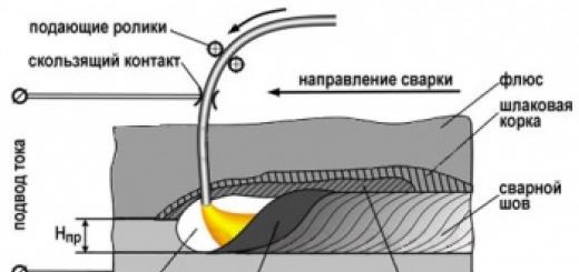
A common disadvantage of compensating voltage stabilizers is their low efficiency due to losses in the transistors of the control element, which, in addition, requires powerful heat sinks that are significantly larger in size and weight than the stabilizers themselves. More progressive technical solution are pulse voltage stabilizers (VST), in which the transistors of the control elements operate in the key mode. When using high-frequency transistors, the problem of efficiency and weight-dimensional characteristics in such stabilizers is solved quite radically.
There are three main ISN circuits: serial ISN of the bucking type (Fig. 12.15), parallel ISN of the boosting type (Fig. 12.16) and parallel inverting type (Fig. 12.17).
All three circuits contain storage choke L, control element 1, blocking diode VD, control elements 2, 3 and filter capacitor C. The buck-type switching series regulator is made according to structural diagram
shown in Fig. 12.15, in which the control element 1 and the inductor L are connected in series with the load Rn. A transistor operating in switching mode is used as a RE. When the transistor is open for a time T„, energy from the input direct current source Ui (or a rectifier with output voltage Uo) is transferred to the load through the inductor L, in which the energy is stored. When the transistor is closed for a time Tp, the energy accumulated in the inductor is transferred to the load through the diode VD. The switching (conversion) period is equal to T=Ti+Tn. Switching (conversion) frequency F=1/T. The ratio of the duration of the open state of the transistor, at which a voltage pulse of duration Ti is generated, to the switching period T is called the duty cycle K3=Ti/T. Thus, in a pulse stabilizer, the regulating element 1 converts (modulates) the input DC voltage Ui into a series of successive pulses of a certain duration and frequency, and a smoothing filter consisting of a diode VD, an inductor L and a capacitor C demodulates them into a DC voltage Uo. When the output voltage Uo or load current Rn changes in the pulse stabilizer using a feedback circuit consisting of measuring element 3 and control circuit 2, the pulse duration changes in such a way that Uo remained unchanged (with a certain degree of accuracy).
The pulsed operating mode makes it possible to significantly reduce losses in the control element and thereby increase the efficiency of the power source, reduce its weight and dimensions. This is the main advantage of pulse stabilizers over continuous compensation stabilizers.
A pulse parallel stabilizer (boost type) is made according to the block diagram in Fig. 12.16, in which the control element 1 is connected in parallel with the load Rn. When the control transistor is open, the current from the power source Ui flows through the inductor L, storing energy in it. Diode VD is in a closed state and therefore does not allow capacitor C to discharge through the open control transistor.
The current into the load during this period of time comes only from capacitor C. At the moment when the control transistor closes, the self-induction emf of the inductor L is summed with the input voltage and the energy of the inductor is transferred to the load, and the output voltage is greater than the input supply voltage Ui. Unlike the diagram in Fig. 12.15 here the inductor is not a filter element, and the output voltage becomes greater than the input voltage by an amount determined by the inductance of the inductor L and the open time of the control transistor (or the duty cycle of the control pulses).
Stabilizer control circuit in Fig. 12.16 is constructed in such a way that, for example, when the input supply voltage Ui increases, the duration of the open state of the control transistor decreases by such an amount that the output voltage Uo remains unchanged.
The pulse parallel inverting stabilizer is made according to the block diagram shown in Fig. 12.17. Unlike the diagram in Fig. 12.16 here the inductor L is connected in parallel with the load Rn, and the control element 1 is connected in series with it. A blocking diode separates the filter capacitor C and the load Rn from the DC control element. The stabilizer has the property of changing (inverting) the polarity of the output voltage Uo relative to the polarity of the input supply voltage. Depending on the control method, the control transistor can be performed with pulse width modulation (PWM), pulse frequency modulation (PFM) or relay control. In PWM stabilizers, the pulse duration Ti changes during operation, but the switching frequency remains unchanged; in PFM stabilizers, the switching frequency changes, but the pulse duration Ti remains constant;
In relay stabilizers, in the process of voltage regulation, both the duration of the pulses and their repetition rate change.
The most widely used in practice is the sequential ISN (Fig. 12.15), in which the storage choke is also an element of the smoothing LC filter. In the stabilizers in Fig. 12.16 and 12.17, inductor L does not participate in smoothing the output voltage ripple. In these schemes, ripple smoothing is achieved only by increasing the capacitance of capacitor C, which leads to an increase in the mass and dimensions of the filter and the device as a whole.
Static control characteristic determined for the stabilizer in Fig. 12.15 according to the formula Uo/Ui=Kз (1 - Kg), is a straight line, the slope of which depends (without taking into account losses in the control transistor and diode) on the ratio of the active resistances of the inductor and the load Kg=Rd/Rn. The load voltage Uo is determined by the relative duration of the control pulses (at constant Ui) and cannot be greater than the supply voltage, and the linearity of this characteristic corresponds to the conditions for stable operation of the ISN.

Let's consider the main elements of the ISN in Fig. 12.15. Let's start with the main block, the diagram of which is shown in Fig. 12.18. The block includes a power section and a regulating element on transistor VT1, controlled by a switch on transistor VT2 (diode VD2 serves to protect the base junction VT2 with a large negative input control signal). The resistance of resistor R1 is selected from the condition of ensuring the closed state of transistor VT1 (100...900 Ohms), and R2 - approximately from the condition kbUi=R2 Ikmax where k=l,5...2 is the saturation safety factor; b, Ikmax - current amplification factor and maximum pulse
The initial data for choosing the circuit parameters in Fig. 12.18 are:
voltage Ui and limits of its change; internal resistance Ri of the source Ui; rated output voltage of the stabilizer Uo and permissible limits of its adjustment; maximum Inmax and minimum Imin load currents, permissible ripple amplitude of the stabilizer output voltage; stabilization coefficient Kn and internal resistance Ro; maximum temperature deviation of voltage Uo, etc. The procedure for selecting parameters is as follows:
1. Select the conversion frequency F (up to 100 kHz, for the model - units of kilohertz) and take approximately efficiency = 0.85...0.95.
2. Determine the minimum and maximum values of the relative duration (duty factor) of the voltage pulse at the filter input:
3. From the condition of maintaining the continuity mode of the inductor currents, we determine it
minimum inductance
4. Calculate the product LC from the given value of the ripple voltage U„
from where we then find the capacitance of the capacitor C.
The LC product determines not only the ripple level, but also the nature of the output voltage transients after the stabilizer is turned on.
In Fig. Figure 12.19 shows the results of simulating the circuit in Fig. 12.18 with the following data: F=1 kHz, K=0.5, Rn=100 Ohm, L=200 mH, C=100 µF (for Fig. 12.19, a) and C=1 µF (for Fig. 12.19, b). As can be seen from the figures, with a relatively large value of the LC product, the transient response of the circuit under study has an oscillatory nature, which leads to output voltage surges, which can be dangerous for the consumer (load).

Let's move on to consider the next functional unit of the ISN - the control circuit and the measuring element.
In this case, it is advisable to consider the characteristics of the modulators used in the ISN.
Switching stabilizers with PWM have the following advantages compared to stabilizers of the other two types:
The possibility of simultaneous synchronization of the conversion frequencies of an unlimited number of ISNs is realized, which eliminates the risk of frequency beats when several ISNs are powered from a common primary direct current source. In addition, when the ISN operates on an unregulated converter (for example, a power amplifier), it is possible to synchronize the frequencies of both devices.
The disadvantage of an ISN with PWM compared to a relay-type stabilizer is that it is more complex circuit control, usually containing an additional master oscillator.
Pulse stabilizers with PFM, while not having significant advantages over other types of ISN, have the following disadvantages:
О the complexity of implementing frequency controllers over a wide range, especially with large changes in supply voltage and load current;
There is no possibility of realizing the above-mentioned advantages of a PWM control system.
The last drawback also applies to relay (or two-position) ISNs, which are also characterized by a relatively large voltage ripple at the load (in stabilizers with PWM or PWM, the output voltage ripple can in principle be reduced to zero, which is impossible to achieve in relay stabilizers).
In the general case, block 3 (Fig. 12.20) contains a voltage divider, a reference voltage source ION, a comparing element and a mismatch amplifier. These elements perform the same functions as in compensating stabilizers. For an ISN with PWM, a synchronizing voltage former (master oscillator) and a threshold device are added to these devices, with the help of which pulses modulated in duration are generated. The duration of the control pulse is changed by modulating its leading or trailing edge.

When the leading edge is modulated, the linearly varying synchronization voltage increases in each period, and when the trailing edge modulates, the control voltage decreases in each period.
When modulating the edges, the synchronization voltage rises and falls at each period. This type of modulation, compared to one-way modulation, makes it possible to implement faster ISNs, since in this case the instantaneous value of the control voltage affects the formation of edges.
the voltage divider and error amplifier gain ratios, respectively; Uy is the amplitude of the synchronizing voltage.
The complete circuit of the ISN with PWM elements is shown in Fig. 12.20. The voltage divider is made on resistors R3, R4, the reference voltage source is on resistor R5 and zener diode VD2, the error signal amplifier is on OU1, the threshold device is on OU2. Since both op-amps are powered from a unipolar source, to match the levels in the key stage, VT2 is included in the emitter circuit parametric stabilizer(VD3, R8). A functional generator in the triangular pulse mode was used as a master; When modulating on a leading edge, the duty cycle is selected as maximum (99%), when modulating on a falling edge - as minimum (0.1%), when modulating on both edges - 50%. In Fig. Figure 12.21 shows the result of modeling the process of generating control pulses during modulation along the leading edge.

Shown in Fig. 12.21 the results were obtained at Rn = 100 Ohm and Ui = 20 V. As can be seen from Fig. 12.21, immediately after turning on the power source, control pulses of maximum duration are formed, then a long pause occurs due to a positive jump in the output voltage Uo, then the forced mode begins again due to a negative jump in Uo. The steady-state mode of control pulse formation occurs after several periods of the master oscillator control signal.
Test tasks
1. For the circuit in Fig. 12.18 obtain the dependence Uo=f(K,) at F=1 kHz, Uy=3 V (unipolarity of the control rectangular pulses is ensured by setting the constant component Offset=3 V on the functional generator, the duty cycle K is set by selecting the Duty cycle parameter), Ui= 30 V, Rn=100 Ohm, L=100 mH, C=100 µF.
2. For the circuit in Fig. 12.18, study the dependence of the shape of transient processes on the active loss resistance Rd, including a resistance of 0.1... 10 Ohm in series with the inductor.
3. Examine the ISN according to the diagram in Fig. 12.20 when modulating the falling edge, simultaneously along the leading and falling edges and compare the results on the time the devices reach steady state.
4. For each method of generating control signals in steady state, obtain the dependence of the period of generating control signals on the load resistance Rn in the range of 10... 1000 Ohms and the input voltage Ui in the range of 15...40 V.
The use of various types of technology in Everyday life is an indispensable attribute of modern society. But not all devices are designed to connect to a standard 220V power supply. Many of them consume energy with voltages ranging from 1 to 25V. To supply it, special equipment is used.
However, its main task is not so much to reduce the output parameters, but to maintain their stable level in the network. This can be solved using a stabilization device. But as a rule, such devices are quite cumbersome and not very convenient to use. The best option- This is a pulse voltage stabilizer. It differs from linear ones not only in dimensions, but also in its operating principle.
What is a pulse stabilizer
A device consisting of two main components:
- Integrating;
- Adjustments.
At the first stage, energy is accumulated with its subsequent release. The control unit supplies current and, if necessary, interrupts this process. Moreover, unlike linear models, in pulsed models this element can be in a closed or open state. In other words, it works like a key.
Pulse device device
The scope of application of such devices is quite wide. However, they are most often used in navigation equipment, and a pulse stabilizer should be purchased to connect:
- LCD TVs
- Power supplies used in digital systems;
- Low-voltage industrial equipment.
Pulse boost voltage stabilizers can also be used in networks with alternating current to convert it to direct current. Devices of this class are also used as power supplies for powerful LEDs, recharging batteries.
How the equipment works
The operating principle of the device is as follows. When the regulating element is closed, energy is accumulated in the integrating element. This causes an increase in voltage. When the switch is opened, electricity is gradually transferred to consumers, leading to a decrease in voltage.
Watch the video and see how the device works:
Such a simple way of operating the device allows you to save energy, and in addition made it possible to create a miniature unit.
The following parts can be used as a regulatory element:
- Thyristor;
- Transistors.
The integrating units of the device are:
- Throttle;
- Battery;
- Capacitor.
The design features of the stabilizer are related to the way it works. There are two types of devices:
- With a Schmitt trigger.
Let's look at the differences between these two types of pulse voltage stabilizers.
PWM models

PWM model
Devices of this type have some differences in design. They consist of two main elements as well:
- Generator;
- Modulator;
- Amplifier.
Their operation is directly dependent on the input voltage, as well as the duty cycle of the pulses.
When the key is opened, energy is transferred to the load and the amplifier is switched on. It compares the voltage values and, having determined the difference between them, transmits the gain to the modulator.
The final pulses must have a duty cycle deviation that is proportional to the output parameters. After all, the position of the key depends on them. At specific duty cycle values, it opens or closes. Since impulses play the main role in the operation of the device, they gave it its name.
Devices with a Schmitt trigger
This type of pulse voltage stabilizer is characterized by a minimal set of elements. The main role in it is given to the trigger, which includes a comparator. The task of this element is to compare the output voltage value with the maximum permissible.
Let's watch a video of the operating principle of a device with a Schmitt trigger:
The operation of the device is as follows. When the maximum voltage is exceeded, the trigger switches to the zero position and opens the key. At the same time, the throttle discharges. But as soon as the voltage reaches a minimum value, it switches from 0 to 1. This leads to the closure of the switch and the flow of current into the integrator.
Although such devices have a fairly simple design, they can only be used in certain areas. This is explained by the fact that pulse voltage stabilizers can be step-down or step-up.
Classification of devices
The division of devices into types is carried out according to various criteria. So, based on the ratio of voltage at the input and output, the following types of devices are distinguished:
- Inverting;
- Randomly changing voltage.
The following parts can be used as a key:
- Transistors;
- Thyristors.
In addition, there are differences in the operation of pulse stabilizers themselves. DC voltage. Based on this, they are classified into models operating on:
- Based on pulse width modulation;
- Two-position.
Advantages and disadvantages of stabilizers

Modular stabilizer
Like any other device, a modular stabilizer is not ideal. It has its pros and cons that you should be aware of. The advantages of the device include:
- Easy to achieve stabilization;
- High efficiency;
- Voltage equalization over a wide range;
- Stable output parameters;
- Compact dimensions;
- Soft start.
The disadvantages of the device include, first of all, its complex design. The presence of a large number of specific elements in it does not allow achieving high reliability. In addition, the disadvantage of a pulsed DC voltage stabilizer is:
- Creation of a large number of frequency interference;
- Difficulty in performing repair work;
- The need to use devices that compensate for power factor.
Allowable frequency range
Operation of this device is possible at a sufficiently high conversion frequency, which is its main difference from devices with a network transformer. Increasing this parameter allowed us to achieve minimal dimensions.
For most models, the frequency range can be from 20 to 80 kHz. However, when choosing both key and PWM devices, you need to take into account the higher harmonics of the currents. In this case, the upper value of the parameter has certain restrictions that meet the requirements for radio frequency equipment.
Application of devices in AC networks
Devices of this class are capable of converting D.C. at the entrance to the same at the exit. If you intend to use them on the network alternating current, then you will need to install a rectifier and an anti-aliasing filter.
However, you should know that as the voltage at the input of the device increases, the output current decreases and vice versa.
Possible using a bridge rectifier. But in this case it will be a source of odd harmonics and the use of a capacitor will be required to achieve the required power factor.
Review of manufacturers
When choosing a stabilizer, pay attention not only to its specifications, but also on design features. The brand of the manufacturer is also important. It is unlikely that a device manufactured by a company unknown to a wide range of buyers will be of high quality.

Smartmodule products
Therefore, most consumers prefer to choose models belonging to popular brands, such as:
- Hobbywing;
- Smartmodule.
The products of these companies are of high quality, reliability and are designed for a long service life.
Conclusion
Usage household appliances and other electrical appliances have become an essential condition for a comfortable life. But in order to ensure that your devices do not fail during unstable power grids, you should think in advance about purchasing a stabilizer. Which model to choose depends on the parameters of the equipment used. If you intend to connect modern LCD TVs, monitors and similar devices, then the ideal option is a switching stabilizer.
In stabilizers with PWM, a generator is used as a pulse element, the pulse or pause time of which varies depending on the constant signal arriving at the input of the pulse element from the output of the comparison circuit.
Operating principle of a PWM stabilizer is as follows. DC voltage from the rectifier or battery is supplied to the regulating transistor, and then through the filter to the output of the stabilizer. The output voltage of the stabilizer is compared with the reference voltage, and then the difference signal is applied to the input of a device that converts the direct current signal into pulses of a certain duration, the latter changing in proportion to the difference signal between the reference and measured voltage. From a device that converts direct current into pulses, the signal is sent to a control transistor; the latter periodically switches and the average voltage value at the filter output depends on the ratio between the time the transistor is in the open and closed states (on the pulse width - hence the name of this type of modulation), and the PWM pulse repetition rate is constant. When the voltage at the output of the stabilizer changes, the direct current signal changes, and therefore the width (duration) of the pulse (at a constant period); As a result, the average value of the output voltage returns to its original value.
In stabilizers with PFM When the signal at the output of the pulse element changes, the duration of the pause changes, but the duration of the pulse remains unchanged. Moreover, unlike stabilizers with PWM, the switching frequency of the control transistor depends on changes in the load current and output voltage, and therefore is a changing, non-constant value - hence the name of this type of modulation. The operating principle of such stabilizers is similar to the operating principle of PWM stabilizers. A change in the output voltage of the stabilizer causes a change in the pause, which leads to a change in the pulse frequency and the average value of the output voltage remains unchanged.
Operating principle of relay or two-position stabilizers are somewhat different from the principle of operation of stabilizers with PWM. In relay stabilizers, a trigger is used as a pulse element, which in turn controls a regulating transistor. When a constant voltage is applied to the input of the stabilizer, at the first moment the regulating transistor is open and the voltage at the output of the stabilizer increases, and the signal at the output of the comparison circuit increases accordingly. At a certain value of the output voltage, the signal at the output of the comparison circuit reaches a value at which the trigger is triggered, closing the control transistor. The voltage at the output of the stabilizer begins to decrease, which causes a decrease in the signal at the output of the comparison circuit. At a certain signal value at the output of the comparison circuit, the trigger fires again, opens the control transistor and the voltage at the output of the stabilizer begins to increase; it will increase until the trigger closes the control transistor again, and thus the process repeats.
A change in the input voltage or load current of the stabilizer will lead to a change in the open state time of the control transistor and to a change in its switching frequency, and the average value of the output voltage will be maintained (with a certain degree of accuracy) unchanged. Thus, as in PFM stabilizers, in relay stabilizers the switching frequency of the control transistor is not constant.
Advantages and disadvantages of the described stabilizers.
1. In principle, output voltage ripple in stabilizers with PWM and PWM may be completely absent, since the pulse element is controlled by the constant component of the control circuit signal; In relay stabilizers, output voltage pulsations must fundamentally take place, since periodic switching of the trigger is possible only when the output voltage periodically changes.
One of the main disadvantages of PWM and PWM stabilizers compared to relay ones is their lower operating speed.
When working with many different technologies, the question is often: how to manage the power that is available? What to do if it needs to be lowered or raised? The answer to these questions is a PWM regulator. What is he? Where is it used? And how to assemble such a device yourself?
What is pulse width modulation?
Without clarifying the meaning of this term, it makes no sense to continue. So, pulse width modulation- this is the process of controlling the power that is supplied to the load, carried out by changing the duty cycle of the pulses, which is done at a constant frequency. There are several types of pulse width modulation:
1. Analog.
2. Digital.
3. Binary (two-level).
4. Trinity (three-level).
What is a PWM regulator?

Now that we know what pulse width modulation is, we can talk about the main topic of the article. A PWM regulator is used to regulate the supply voltage and to prevent powerful inertial loads in automobiles and motorcycles. This may sound complicated and is best explained with an example. Let’s say you need to make the interior lighting lamps change their brightness not immediately, but gradually. The same applies to side lights, car headlights or fans. This desire can be realized by installing a transistor voltage regulator (parametric or compensation). But with a large current, it will generate extremely high power and will require the installation of additional large radiators or an addition in the form of a forced cooling system using a small fan removed from the computer device. As you can see, this path entails many consequences that will need to be overcome.
The real salvation from this situation was the PWM controller, which works on powerful field power transistors. They can handle high currents (up to 160 Amps) with only 12-15V gate voltage. It should be noted that the resistance of an open transistor is quite low, and thanks to this, the level of power dissipation can be significantly reduced. To create your own PWM controller, you will need control circuit, which can provide a voltage difference between the source and gate within the range of 12-15V. If this cannot be achieved, the channel resistance will greatly increase and the power dissipation will increase significantly. And this, in turn, can cause the transistor to overheat and fail.
A whole range of microcircuits for PWM regulators are produced that can withstand an increase in input voltage to a level of 25-30V, despite the fact that the power supply will be only 7-14V. This will allow the output transistor to be turned on in the circuit along with the common drain. This, in turn, is necessary to connect a load with a common minus. Examples include the following samples: L9610, L9611, U6080B ... U6084B. Most loads do not draw more than 10 amps of current, so they cannot cause voltage sags. And as a result, you can use simple circuits without modification in the form of an additional unit that will increase the voltage. And it is precisely these samples of PWM regulators that will be discussed in the article. They can be built on the basis of an asymmetrical or standby multivibrator. It’s worth talking about the PWM engine speed controller. More on this later.
Scheme No. 1

This PWM controller circuit was assembled using CMOS chip inverters. It is a rectangular pulse generator that operates on 2 logic elements. Thanks to the diodes, the time constant of discharge and charge of the frequency-setting capacitor changes separately here. This allows you to change the duty cycle of the output pulses, and as a result, the value of the effective voltage that is present at the load. In this circuit, it is possible to use any inverting CMOS elements, as well as NOR and AND. Examples include K176PU2, K561LN1, K561LA7, K561LE5. You can use other types, but before that you will have to think carefully about how to correctly group their inputs so that they can perform the assigned functionality. The advantages of the scheme are the accessibility and simplicity of the elements. Disadvantages are the difficulty (almost impossibility) of modification and imperfection regarding changing the output voltage range.
Scheme No. 2

Possesses best characteristics than the first sample, but more difficult to implement. Can regulate the effective load voltage in the range of 0-12V, to which it changes from an initial value of 8-12V. Maximum current depends on type field effect transistor and can reach significant values. Considering that the output voltage is proportional to the input control, this diagram can be used as part of a control system (to maintain temperature levels).
Reasons for the spread
What attracts car enthusiasts to a PWM controller? It should be noted that there is a desire to increase efficiency when constructing secondary electronic equipment. Thanks to this property, this technology can also be found in the manufacture of computer monitors, displays in phones, laptops, tablets and similar equipment, and not just in cars. It should also be noted that the this technology when used. Also, if you decide not to buy, but to assemble a PWM controller yourself, you can save money when improving your own car.
Conclusion

Well, you now know what a PWM power regulator is, how it works, and you can even assemble similar devices yourself. Therefore, if you want to experiment with the capabilities of your car, there is only one thing to say about this - do it. Moreover, you can not only use the diagrams presented here, but also significantly modify them if you have the appropriate knowledge and experience. But even if everything doesn’t work out the first time, you can gain a very valuable thing - experience. Who knows where it might come in handy next and how important its presence will be.
This circuit is a step-down regulator with the ability to regulate and protect or limit the current. A special feature of the device is its use in the power section bipolar transistor with static induction (BSIT) and TL494 microcircuits with two operational amplifiers. Op-amps are used in the negative feedback circuit of the regulator, ensuring optimal operation.
Operating parameters of the regulator:
- rated supply voltage – 40…45V;
- range adjustable voltage output – 1…30V;
- PWM controller frequency – 40 kHz;
- regulator output circuit resistance – 0.01 Ohm;
- long-term maximum output current is 8A.
The stabilizer circuit is shown in Figure 1. A smoothing filter made of capacitors C16-18, storage inductance L1, diode-discharger VD6, switch VT1 make up the power circuit of the device. The construction of the power circuit is classic, the difference is the additional elements C5, VDD1, R7, VT2, designed to ensure safe operation of the power switch (VT1). Transformer T2 allows you to reduce the rate of current increase when opening the VT1 switch. The energy accumulated when closing the key goes to the input of the circuit through the right side diode assembly VD1. Capacitance C5 is designed to reduce the rate of voltage rise across the switch. Installation of OBR circuit elements optimizes the operating mode of the key transistor, reducing heat losses and shock loads. The protection of the VT1 key from the effects of reverse current through the C5T2 circuit is provided by the VD1 diode located on the left.
Picture 1
The control signal to the switch gate is supplied through the isolation transformer T1, the primary winding of which is connected to the collector circuit of transistor T2. Elements R1, VD2, VD3 are designed to limit surges in the reverse voltage of the switch gate. The VT2 emitter is connected through a limiting resistor R8 to pins 8 and 10 of the DA1 microcircuit (collectors of the output transistors). The limiting resistor allows you to select the optimal value of the gate current of the VT1 switch.
The operation of the circuit is controlled on a specially designed TL494 chip. The connection principle is classic, pins 7 and 13 are connected, single-ended mode. To be able to work with a minimum voltage, pin 2 is set as a divider reference voltage approximately 0.9V. The voltage on the 4th leg determines the maximum duty cycle of the generated pulses. The amplitude-frequency response of the circuit is time-corrected by the master chains C12R14, C11R13. The generation frequency is set by the C14R21 chain. Negative voltage feedback is established by elements VD8, R20, R25, R24. The voltage at the output of the stabilizer is set variable resistance R24. Current control is performed by the voltage drop across resistors R5, R4 installed in parallel. The signal from them goes to the 2nd operational amplifier control microcircuit (contacts 16,15). The maximum current limitation at the device output is adjusted by resistance R19.
The op-amp of the DA2 chip is designed to protect the device when the output current exceeds the maximum permissible. The inputs of op-amp DA1 and op-amp DA2 are connected to a current sensor using resistors R5, R4. When the voltage drop across the sensor increases, the output of the comparator will appear high voltage. Through the closed contact SA1, a positive feedback chain is formed; the high voltage will maintain op-amp DA2 in this state and block the operation of DA1 through input 16.
Switch SA1 in the open state ensures operation of the device with maximum current limitation. The HL1 LED lights up when the load is disconnected or when the current is limited.
The power supply for the control part of the circuit is provided by a stabilizing chain of elements C6-10, C4, C3, R3, R2, VD5, VD4, VT2.
The device is assembled on a fiberglass board with foil on one side. Remote parts:
- switch SA1;
- LED HL1;
- voltage regulator
All tracks intended for the power part of the circuit should be further strengthened copper wire cross section of at least 1mm 2. Parts can be used Russian production or their foreign analogues. The heat sink area for the key transistor and diode assembly VD1 is at least 370 cm 2, for VD6 - at least 130 cm 2.